
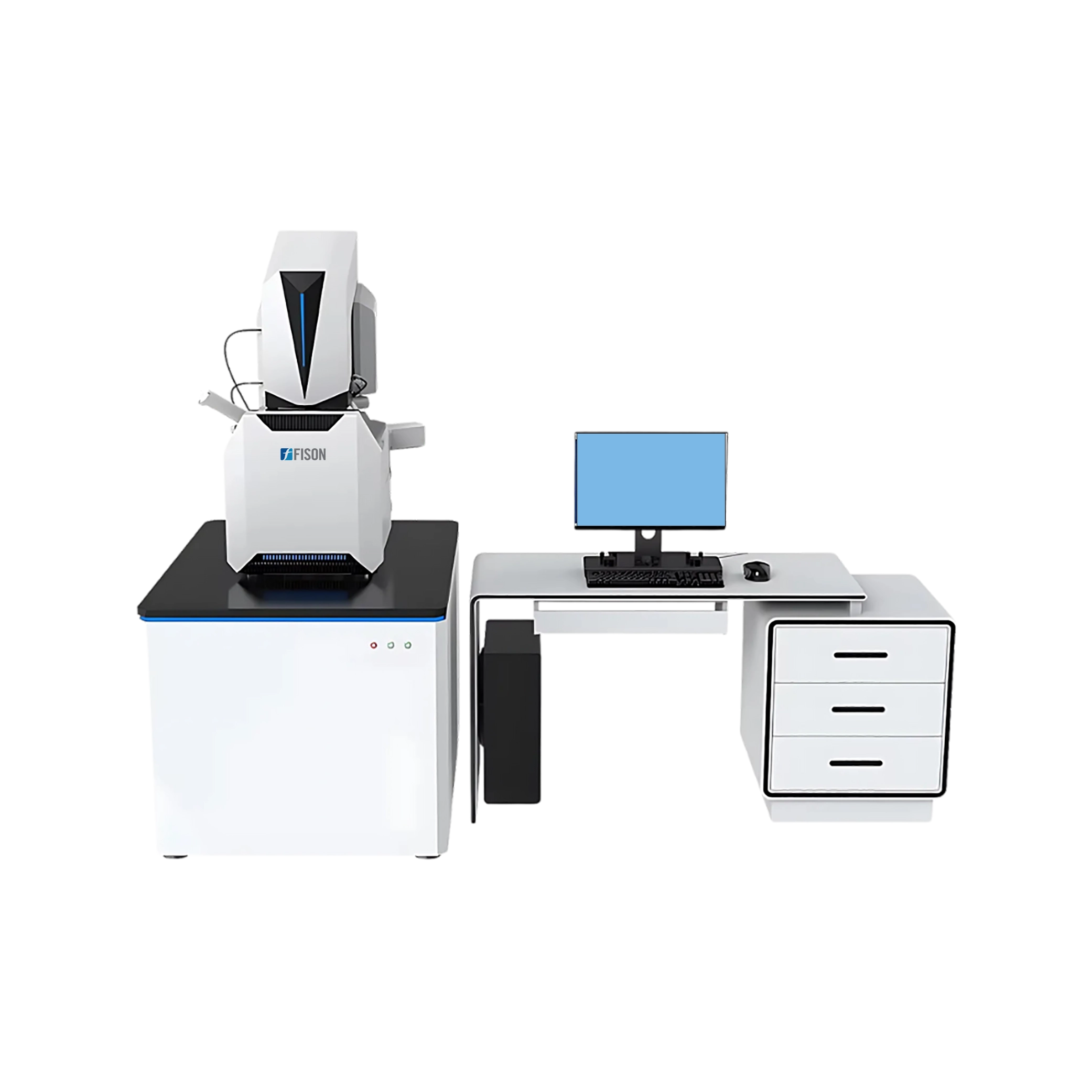
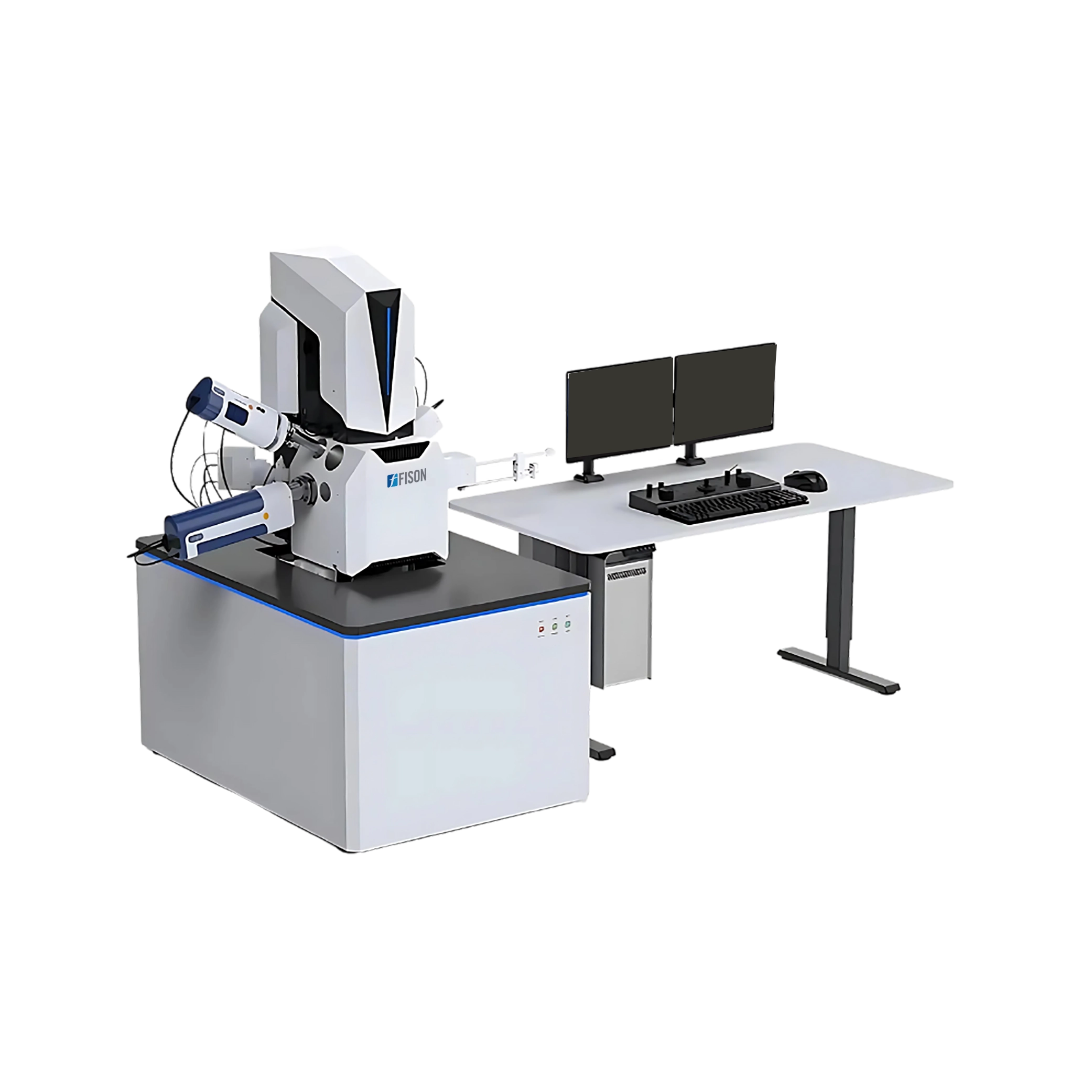
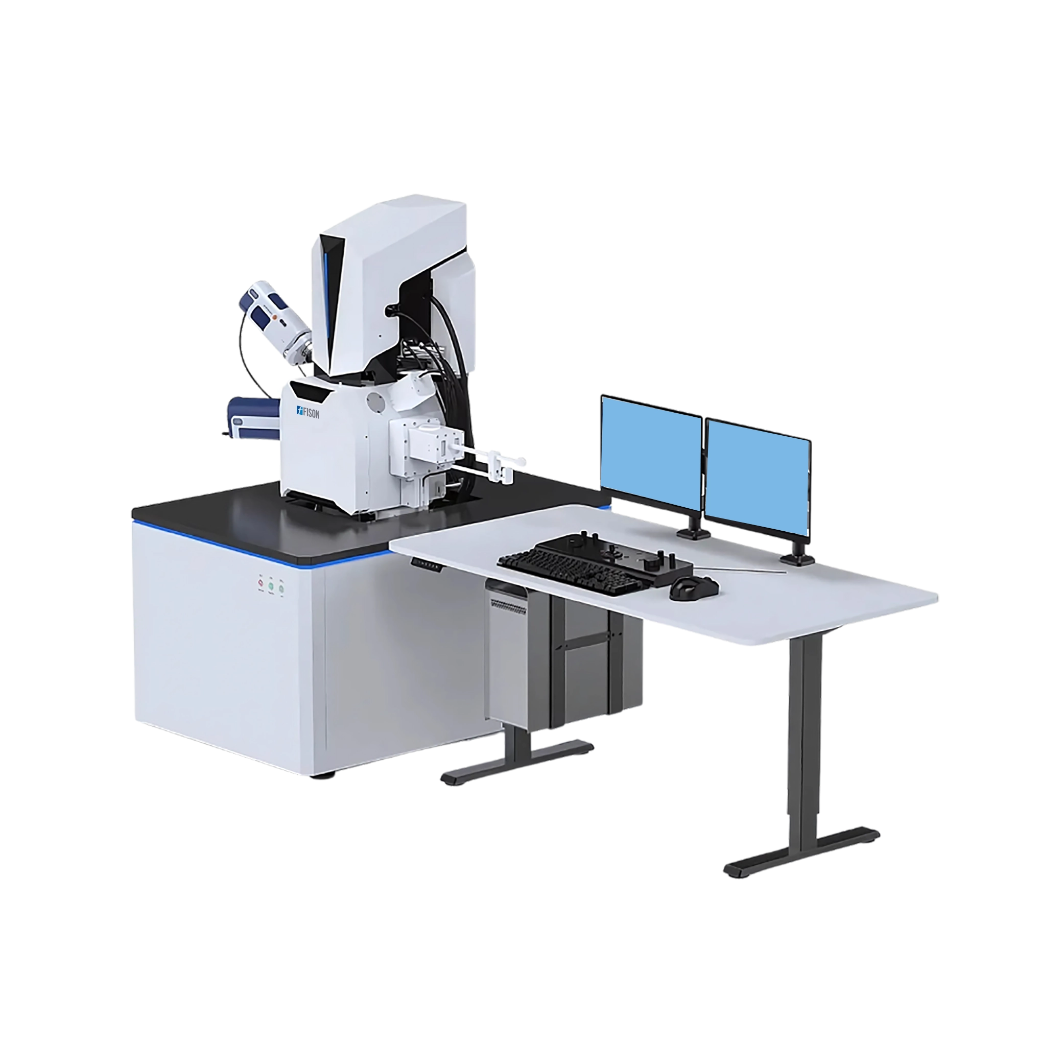
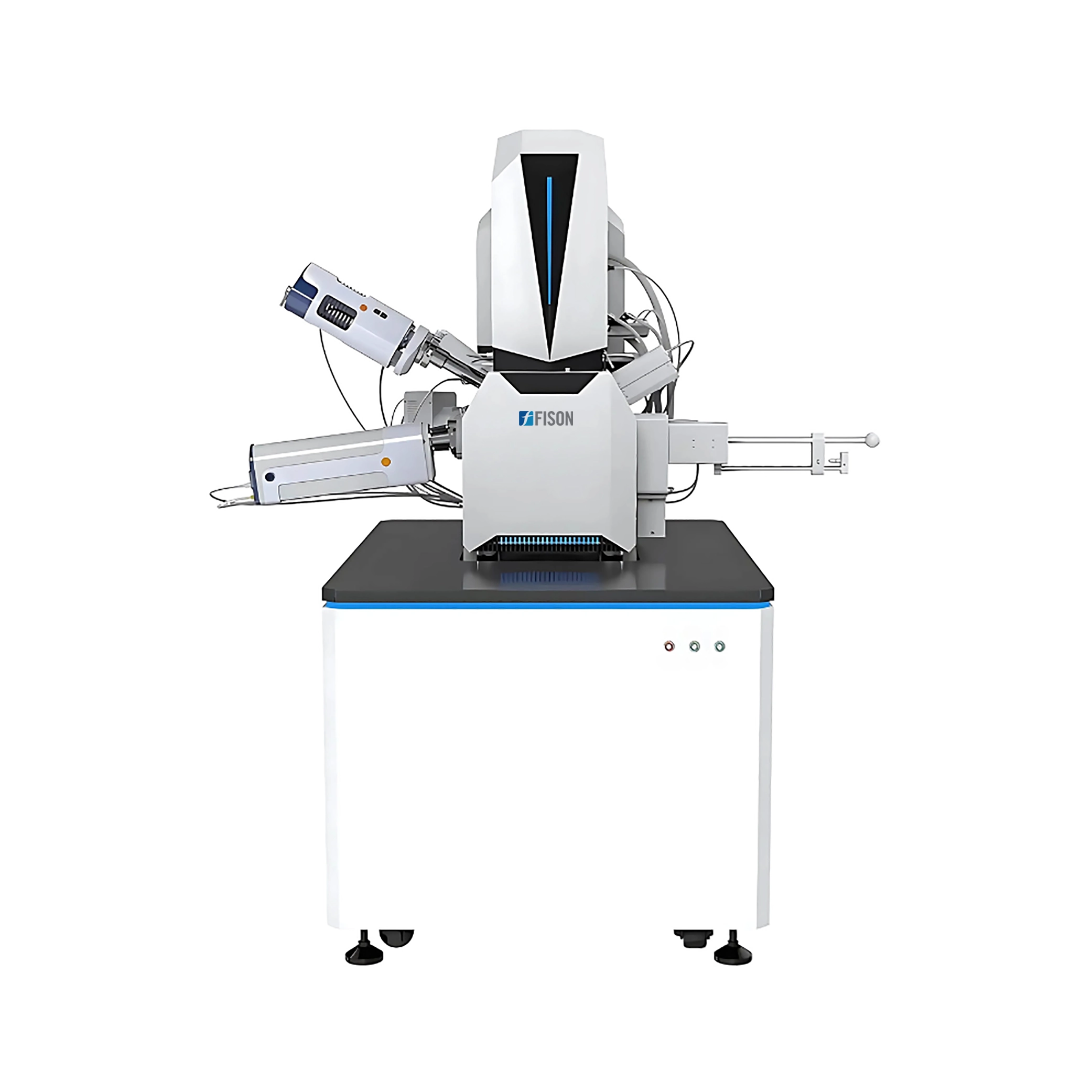
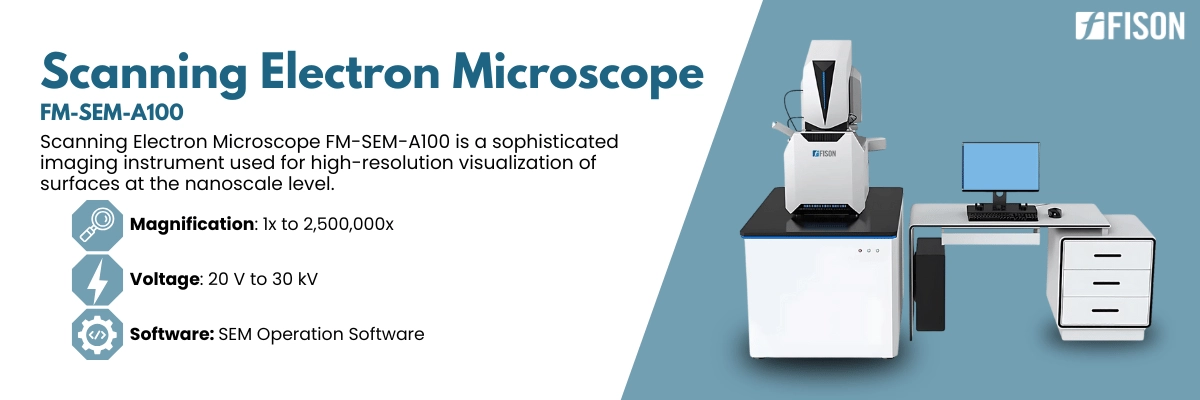
Scanning Electron Microscope FM-SEM-A100 is a sophisticated imaging instrument used for high-resolution visualization of surfaces at the nanoscale level. Equipped with Schottky Field Emission Electron Gun, with in cylinder Deceleration. It uses a focused beam of electrons to scan the specimen's surface. It has five axis automatic working stage.
$622,500.00
| Magnification | 1x to 2,500,000x |
| Resolution | 1.0 nm at 15 kV (SE), 1.5 nm at 1 kV (SE), 0.8 nm at 30 kV (STEM) |
| Voltage | 20 V to 30 kV |
| Electron Gun | Schottky Field Emission Electron Gun, In- cylinder Deceleration, Electromagnetic Composite Objective, Water-cooled Thermostatic Objective |
| Vacuum System | Type - Fully Auto Control Oil Free Vacuum Sample Room pressure - < 5×10⁻⁴ Pa Electron Gun pressure |
| Vacuum Pump | Mechanical pump flow rate - > 6 m3/h Turbo molecular pump flow rate - > 240 L/s Ion pump flow rate - >25 L/s |
| Working Stage | 5 Axes Auto Stage, X:120 mm, Y:115 mm, Z:50 mm, T: -10° to + 90°, R: 360° |
| Camera | Vertical Optical Navigation CCD, Horizontal Monitoring CCD |
| Detector | Secondary Electron Detector (ETD), High Angle Electron Detector In lens |
| Software | SEM Operation Software |
| Display | Multi-Channel Display |
| Navigation | Gesture navigation |
| Image enhancement features | Auto Brightness Contrast, Auto Focus, Auto Astigmatism |
| Image format support | TIFF, JPG, BMP, PNG |
| Computer specification | Working Station, Memory: 16 G, Hard Disk: 512 G, 24-inch Monitor, Win10 operating system |
| Installation Room | Dimension (L×W×H) - 3000×4000 ×2300 mm Temperature - 20 to 25 ℃ Humidity - < 50% |
| Power Supply | AC 220 V (±10 %), 50 Hz,2 kVA |
| packaging dimension (L×W×H) | 180 × 160 × 200 cm |
| Net weight | 400 kg |
| Gross weight | 950 kg |
| Accessories no | Name | Quantity |
| 1 | BSE Back Scattering | 1 |
| 2 | EDS Energy Dispersive | 1 |
| 3 | EBSD, Electron Beam Backscattered | 1 |
| 4 | EBSD Bruker Quantax e-Flash | 1 |
| 5 | EDS+EBSD, Electron | 1 |
| 6 | STEM | 1 |
| 7 | EBIC, Electron Beam | 1 |
| 9 | Knob Control Panel &Trackball | 1 |
| 10 | Sample Exchange | 1 |
| 11 | Beam Gate & Electron | 1 |
| 12 | Low Vacuum Detector (LV Module, Work With BSE) | 1 |
| 13 | Double Anode (Tetrode) | 1 |
| 14 | Tungsten Filament | 6 pcs in one box |
| 15 | Large Size Image Stitching Software | 1 |
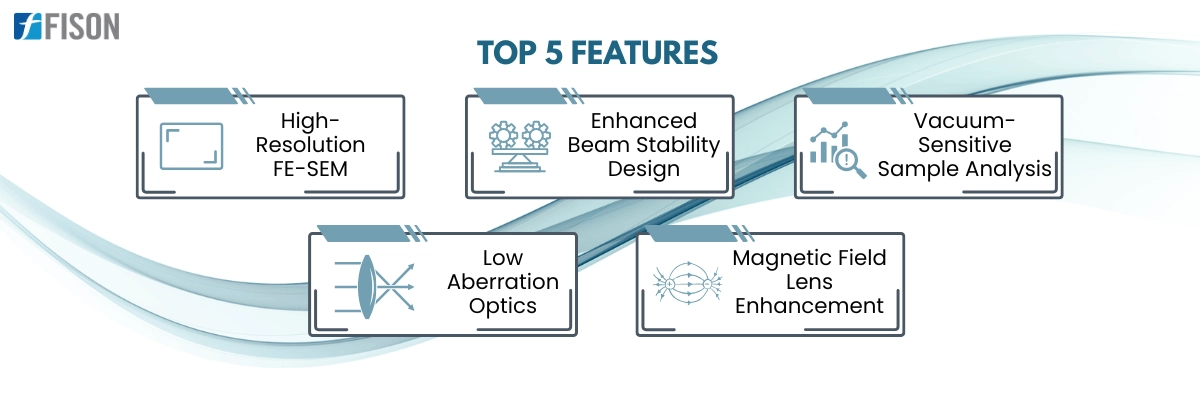
Fison Scanning Electron Microscopes are non-destructive and capture high-resolution images down to 0.8 nm. It offers up to 2.5-million-fold magnification via precision electromagnetic lenses. Equipped with auto-operated oil free vacuum system for contamination-free, maintenance-free working environment. It features multi-digital display with advanced camera and diverse application software. Our Scanning Electron Microscopes are experts in surface topography mapping of nanomaterials, biological samples and much more.